Search Results for:

Home >> Search results for""

Apprenticeship Scheme

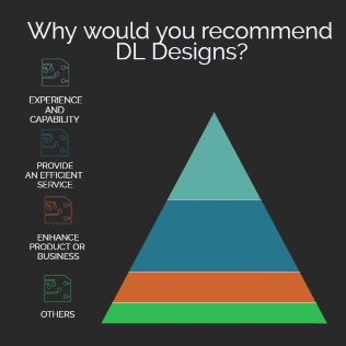
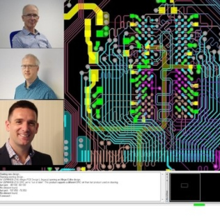
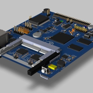
Interested in Electronics? At DL Designs, we have just launched our new apprenticeship scheme. This will help develop you to be best you can be whilst learning on the job. Most of your learning will be on the job and we will support and work with you towards obtaining your qualification at the same time. You'll receive a paid salary just like a normal employee and have dedicated time to study throughout the week. PCB Design combines mechanical expertise with electronic principles.With the combination of attending college and working at DL Designs, we will continue to upskill and motivate you to give you the opportunity to design bespoke PCB layouts for all industries. As an apprentice you will enjoy:Learning the skills from the ground up with a dedicated mentor.Paid salary that will increase through performance reviews.Studying at an accredited college or university.Working with the latest software to help you create innovative and ground breaking PCB designs.Design bespoke PCBs for exciting industries: Space exploration, Transportation, Defence and Security, Telecoms. With our apprenticeship, this is the start of an exciting career in the electronics industry.We are looking for willingness, passion and motivation.With this we will help build your skills to work with us in a fast dynamic environment.We will help you grow the skills you already have and give you the opportunity to meet and work with our diverse stakeholder community. Click to apply or find out more information https://youtu.be/uWh0ZFh07QM

pcb design guide

How to create a PCB Layout Creating the files for a PCB design can be complicated and it's important each stage is completed accurate to ensure there are no issues with the files that are used for manufacturing the PCB. This guide demonstrates the latest process of how to create a PCB design using the best software, this can be built by any circuit board manufacturer. We've created a basic guide of how to create a PCB design.  Click here to read this first. Potential problems, issues and challenges will be addressed. We will also provide cutting edge solutions to prevent complications whilst designing the PCB layout. One of the best tools to use e.g, Cadance, Allegro will be used to show the design cycle. There are some useful online videos available to explain this further. Schematic Drawing the PCB schematic is fundamental as designing the PCB itself. The schematic is used to place all of the parts and add the connections. Once completed, the schematic will create the PCB layout, adding the components and signals. To start working on the schematic, click on page 1. Right-click on New Page to add additional pages.   Adding all of the parts together before you begin is the best way to avoid missing any components whilst adding the connections. Schematic symbols can be obtained from the libraries provided by Orcad. For the schematic to load the component to the design, the correct footprint has to be assigned. It is essential to follow an IPC naming convention such as IPC-7351. Click on the link to learn more about this. At this point, further part information such as part numbers, values and packages must be provided. The more information that can be added, the more detailed parts lists and other reports can be generated. Once all of the symbols have been added to the schematic and the correct footprint names have been assigned, the connections can be added. Drawing the wires accurately is essential to creating the PCB design. Before the PCB layout can be created, the schematic needs to be assured to help identify any errors are not carried on the design. Adding the connections is very straight forward. Power and ground symbols can be added to simplify the schematic. It's easy to run out of room whilst building the schematic. Keep groups of components close together but away from other groups, whilst…

Process Flow

Initial Concept Explore the requirements and challenges to bring the idea to reality. At DL Designs, we can meet these challenges and make improvements to enhance capabilities.   Schematic Capture Building upon the concept from the ground up starts with the schematic. With all of the correct information, the schematic is used to guide the process and generate key information.   Library Maintenance An area that is often overlooked and can end with manufacturing complications. Our footprints are built to IPC 7351 standard with 3D models assigned by the manufacturer.   PCB Layout Today's technology is evolving faster to enhance how we live. Using the best techniques to create a PCB design to meet the requirements of the concept is vital. Chip manufacturers demand more from PCB layouts to ensure precise functionality.   Manufacturing and Assembly The options available to build the concept are endless. Quality, capabilities, timescales, costs have to be prioritised. Tried and tested partners of DL Designs can find the right solution for you and your product.   Testing Inexpensive prototypes allows the design to examined.  This is arguably the most important board the engineer will work with.  Feasibility studies are crucial to to avoid time lost and expensive PCB coasters.  

Latest News / Blog

[bdp_post_list show_author="false" show_tags="false" show_category="false" media_size="medium" limit="10"]

What do our customers say?

After running a survey to our customers, we were happy to see how satisfied they were and why 90% of our new business is through recommendation. DL Designs takes all feedback onboard and continues to develop to suit the needs of our customers.

Software

Using the right tools is important to complete complex layouts as accurately as possible. It is important to use software to suit our customer's needs, to show how the layout is progressing and how the completed design will appear

Engineering Capability

We have design engineers to build your product from an idea or support your engineering team. As we work as a group we can help deliver a faster turn key solution.  We can arrange production with our trusted suppliers as well.

Video Consultation

Using online business platforms is a great way to share ideas for new projects and observe progress on current designs. Exploring the design with our team often helps to maximise potential. On the flip side, video conferencing is essential for interpreting any problems that may occur.

Signal Integrity

With the advancement of technologies in the electronics industries, high speed signals and increasing complexity is more common place. The importance of a methodical design is crucial for a fully functioning PCB. DDR memory, PCI-E, Gigabit Ethernet are some of the intricacies we take into consideration with how they function and how their environment functions with them.

Layout Expertise

PCB layout is the main bedrock of DL Designs. With a combination of over 100 years of experience and over 7000 designs, DL Designs creates all types of designs to suit all industries. We have a finely tuned system of working to ensure the PCB meets expectations and allows customers to have valuable input. We liaise with manufacturing companies to facilitate the requirements of processors and complex circuitry into our design flow.