
How to create a PCB Layout
Creating the files for a PCB design can be complicated and it’s important each stage is completed accurate to ensure there are no issues with the files that are used for manufacturing the PCB.

This guide demonstrates the latest process of how to create a PCB design using the best software, this can be built by any circuit board manufacturer.
We’ve created a basic guide of how to create a PCB design. Click here to read this first.
Potential problems, issues and challenges will be addressed. We will also provide cutting edge solutions to prevent complications whilst designing the PCB layout.
One of the best tools to use e.g, Cadance, Allegro will be used to show the design cycle. There are some useful online videos available to explain this further.
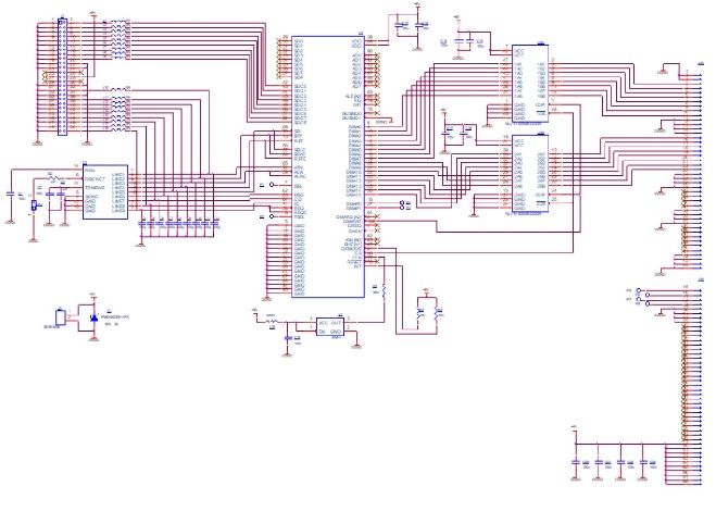
Schematic
Drawing the PCB schematic is fundamental as designing the PCB itself. The schematic is used to place all of the parts and add the connections.
Once completed, the schematic will create the PCB layout, adding the components and signals.

To start working on the schematic, click on page 1. Right-click on New Page to add additional pages.
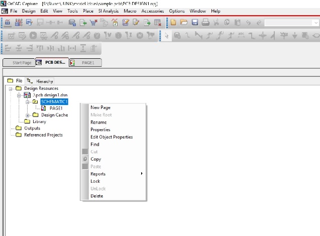
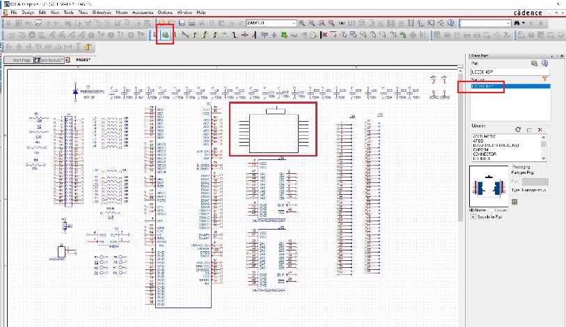
Adding all of the parts together before you begin is the best way to avoid missing any components whilst adding the connections. Schematic symbols can be obtained from the libraries provided by Orcad.
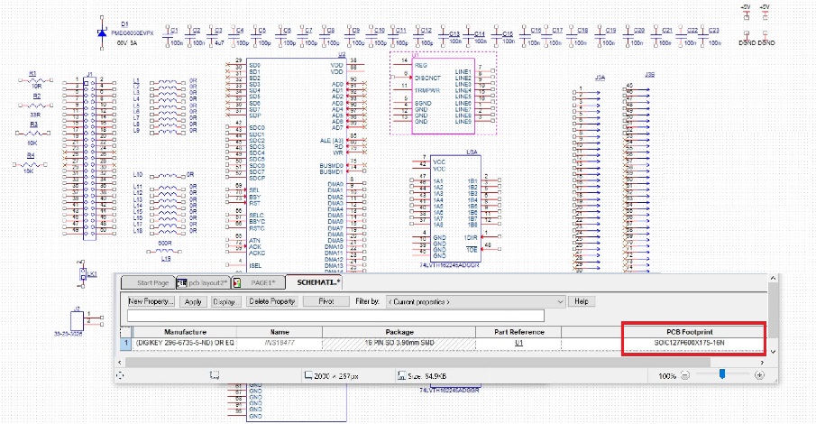
For the schematic to load the component to the design, the correct footprint has to be assigned. It is essential to follow an IPC naming convention such as IPC-7351.
Click on the link to learn more about this. At this point, further part information such as part numbers, values and packages must be provided. The more information that can be added, the more detailed parts lists and other reports can be generated.
Once all of the symbols have been added to the schematic and the correct footprint names have been assigned, the connections can be added. Drawing the wires accurately is essential to creating the PCB design.
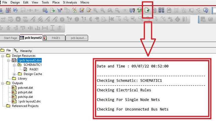
Before the PCB layout can be created, the schematic needs to be assured to help identify any errors are not carried on the design.

Adding the connections is very straight forward. Power and ground symbols can be added to simplify the schematic.

It’s easy to run out of room whilst building the schematic. Keep groups of components close together but away from other groups, whilst adding the connections.

Once the schematic is complete, the PCB design can now be created.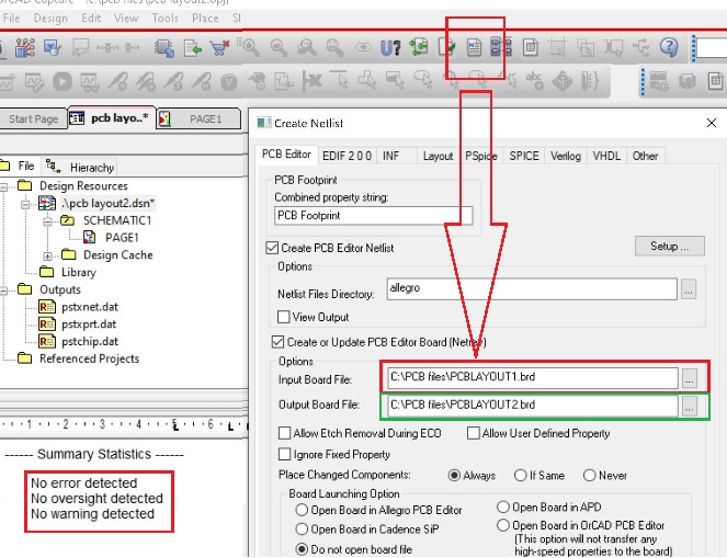
Generating components
Using a start-up layout that is suitable for all of our designs, enter the path of the current design. The Output Board File should be the new file name, usually with the next iteration. Click OK to create the new PCB layout.
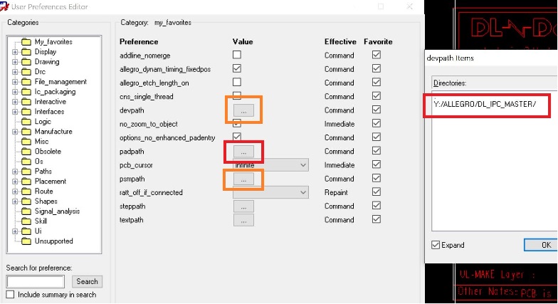
For the layout to import the parts as chosen by the schematic, the library path has to be entered into “devpath”, “pad path” (this contains the pad information), and “psmpath”.
Sometimes more than one library is used for parts, but the primary library should be the first on the list.
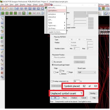
Click quick place to import all of the parts. A board outline has to exist before the parts can be added. The details of added and missing parts are shown. If the part is not placed, it either doesn’t exist or there could be a different number of pins compared to the schematic.
In the above example, one of the parts is not imported onto the PCB design.
The schematic gives details of the missing part.

The datasheet provided by the supplier give enough information to define the padstack, body size, height and orientation.
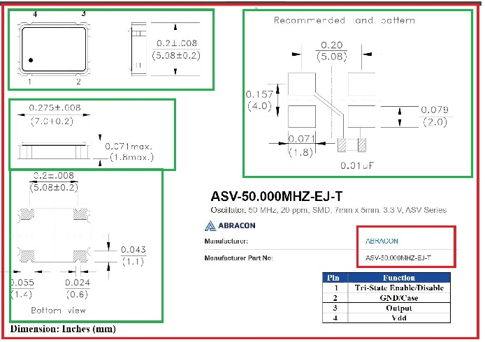
By selecting the correct pad stack and adjusting the grid correctly. The oscillator can be accurately made to add to the PCB layout.

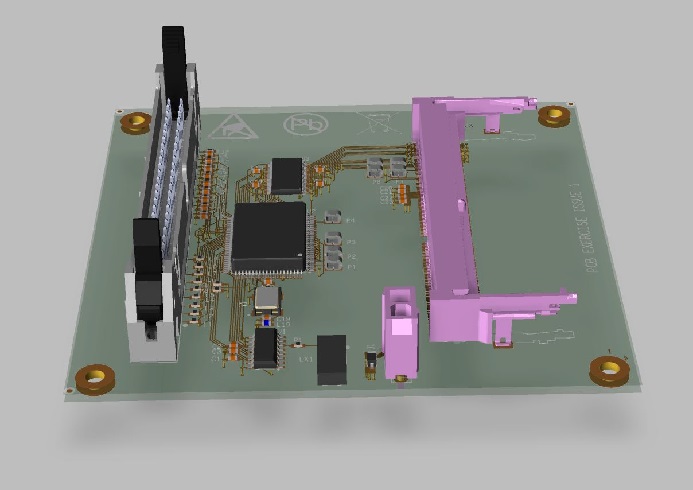
3D models are provided by the manufacturer. Using 3D models can help engineers to visualise the PCB design before manufacturing. This is useful to identify mechanical issues before the circuit board is built.
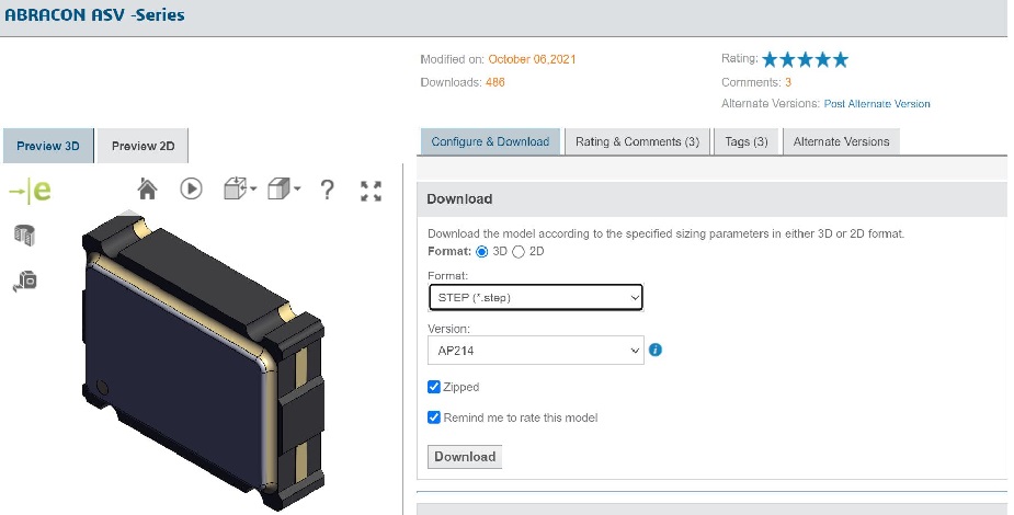
The step model can be downloaded and imported directly onto the component.
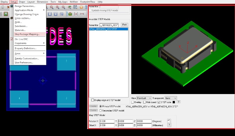
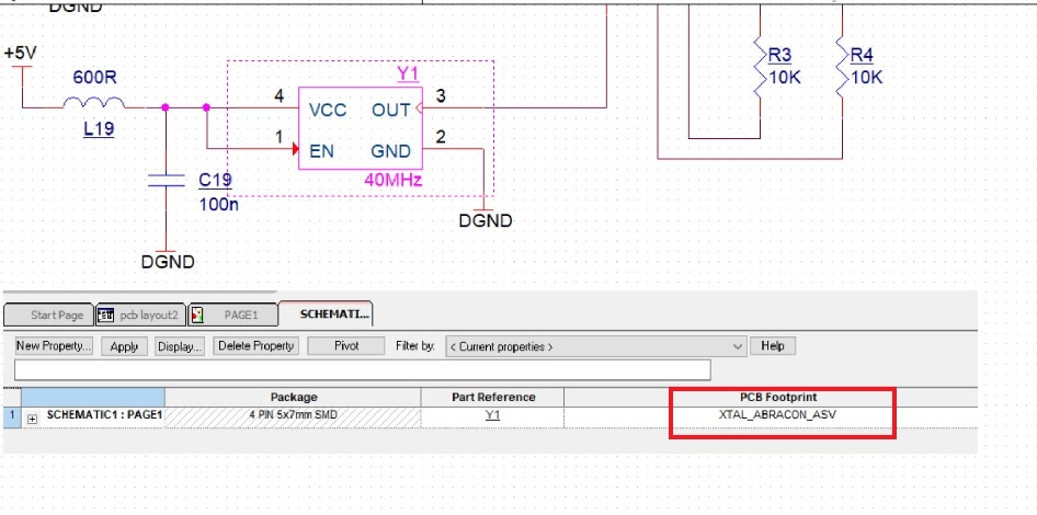
Once the footprint name has been updated and the schematic has rerun the PCB. All of the parts are now on the PCB layout.

Placement stage
During this placement stage, it is important to prioritise the components. Connectors are usually in a fixed position and should be added accordingly. In our example, connectors are on either side of the PCB design, the ICs and discretes (capacitors, resistors, inductors) will be placed in the middle of the circuit board.
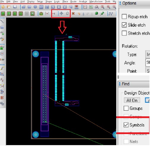
The next area to work on is the group placement. Using the schematic as a guide, the parts should be placed into groups.

Again prioritising the components is important. Decoupling capacitors should be kept as close to the IC as possible. Depending on the type of PCB layout we’re working with, the priority of component placement may differ.
Creating groups of components are square blocks can be important. PCB designs are often compact, saving space can help for the tracking stage later.
As PCB designs become more complex, it is important to read manufacturers datasheets and pay attention to how components affect the rest of the PCB layout. Click here to read about power supplies.

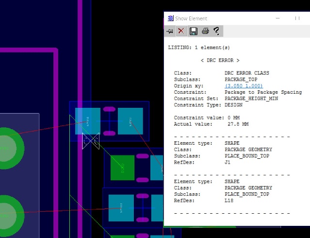
For complex PCB designs, there are lots to think about and it is important to check the placement in case any parts are out of place. Running a DRC check and 3D model can help.
Routing stage
The PCB layout will eventually be sent to a manufacturer to be built and populated with the components that have been selected.
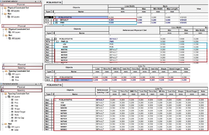
Standard gap and track rules such as 0.2mm are a good starting point. All manufacturers can build to this standard. Complete PCB layouts will have different rules to adhere to, depending on their design functionalities.

There are many ways to start routing the PCB. There are many options to adjust the tracking as the PCB is routed. Changing the vias, track width, the angle are some of the simpler commands.

As all PCB layouts are unique, they have various requirements prioritising the important tracking is a good start to ensure there is enough space and the demands are met.
In the above diagram, the data signals need to run from the controller through the transceiver and onto the connector as short as possible.
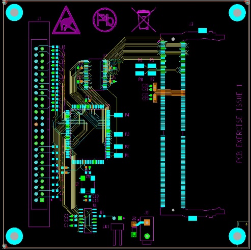

Errors can easily creep into PCB designs. Running a DRC before Gerber files are created is vital. If errors are carried onto the manufacturer, costly faults WILL occur.
Creating gerber files
Now all of the parts, placement, and tracking have been approved and checked. The gerber files can now be created. There are a number of processes involved prior to this.
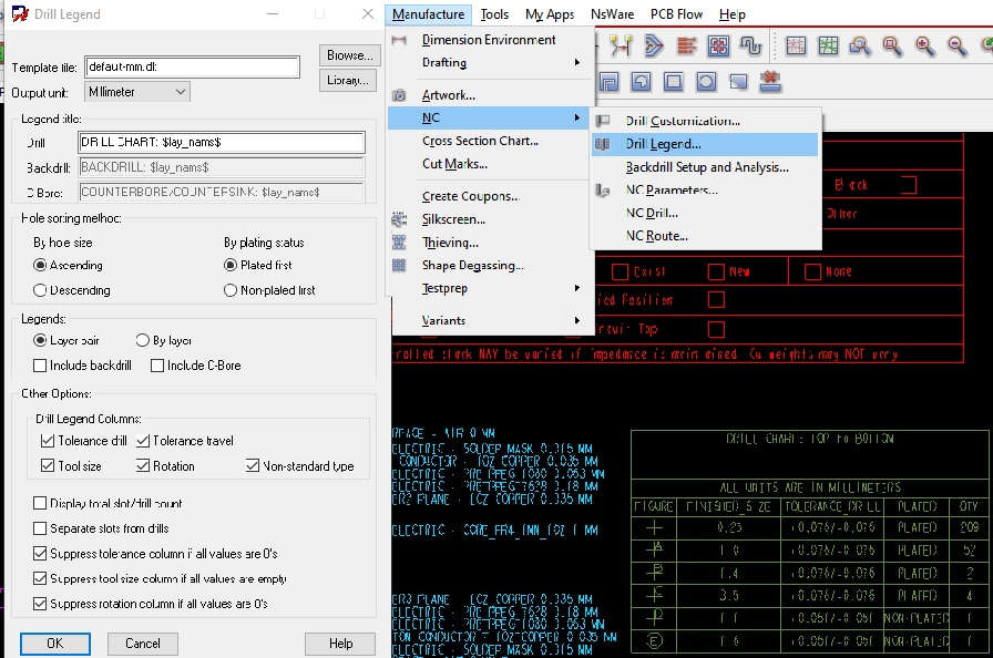
Setting up the drill information is vital for the manufacturer to drill the correct holes through the PCB. Component manufacturers specify the hole size and this must be followed. Depending on the PCB manufacturer, hole tolerances and symbols are shown to detail the specified holes on the PCB.
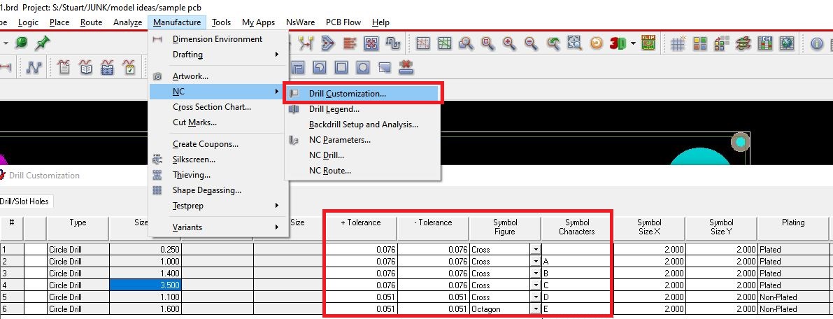
The drilling symbols can be shown on the PCB design and a drill legend is added to identify the hole size.

Each of the layers used to manufacture the PCB is generated. Using reputable PCB layout software such as Allegro makes life easier. Creating the artworks for each layer is straightforward, select the appropriate layers and “Create Artworks” isn’t any easier.

Another benefit to using Allegro, it can generate all sorts of information that will ultimately help the manufacturer and benefit your customer. Mechanical drawings such as step files can help engineers simulate how the circuit board fits within its environment. It can also highlight overlooked errors that can occur in complicated assembly. ODB files are an alternative to Gerber files that some manufacturers may prefer.
By following the correct processes, techniques and using the latest software. PCB layouts can be a pain-free procedure that enhances the product and benefits the design engineer and deliver a good customer experience.

